1 Introduction
This tutorial provides a step-by-step introduction to designing and simulating a simple analog inverter using the open-source tools hosted on the IIC-OSIC platform, specifically with the IHP SG13G2 PDK. The analog inverter, though simple, is a crucial element in analog and mixed-signal circuit design, offering valuable insights into device behavior, biasing, and small-signal performance. The goal of this tutorial is to prrovide a concise overview of the steps needed to create and verify simple CMOS circuits and systems.
2 Full design flow using IIC-OSIC tools
2.1 Schematic entry using Xschem
Schematic entry is performed using Xschem, a powerful open-source schematic editor well-suited for analog and mixed-signal circuit design. In this step, the analog inverter circuit is constructed by placing and connecting NMOS and PMOS transistors from the IHP SG13G2 PDK library. Xschem provides an intuitive interface for defining circuit topology, assigning device parameters like W/L ratios, and labeling nodes for simulation. Proper hierarchy and net labeling ensure compatibility with simulation and layout tools used later in the design flow.
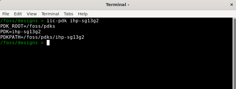
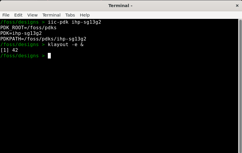
Start terminal and run IIC-OSIC docker image
To select the PDK, use command
iic-pdk ihp-sg13grefer Figure 11
Start xschem and create a new schematic. Name it as (Analog_Inverter.sch)
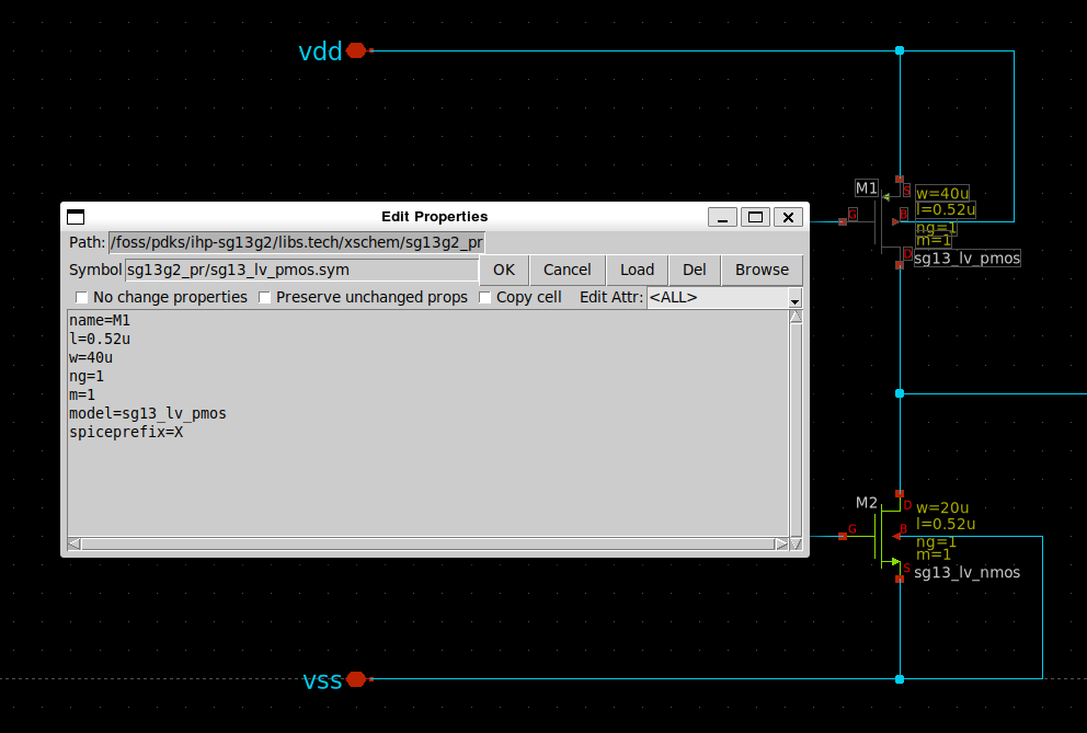
Using
Ctrl+iinsert symbol from the sg13g2 library for lv_nmos and lv_pmos where lv stands for low-voltagecustomize the transistor’s dimensions (select the symbol, right click on it and edit its properties) refer Figure 2
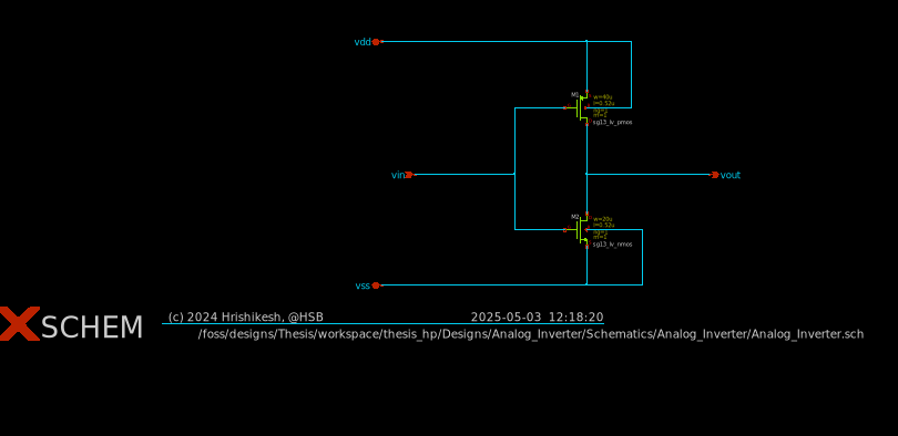
Place an input pin
ipin.symand an output pinopin.symthe symbols are available in the library~/foss/tools/xschem/share/xschem/xschem_library/deviceslabel the name of the input and output pins (select the pin, right click on it and edit its properties)To wire to components,
Ctrl+wOnce finished, save the schematic
Ctrl+Shift+SSee Figure 4
- For creating a symbol,
Symbol --> Make symbol from schematic | Ctrl+L. We can also edit the symbol by opening it in a new tab, see Figure 4

- Now that we have created a symbol, we need to perform DC and Transient analysis using NgSpice.
2.2 Simulation using NgSpice
To perform various analysis, we need to create simulation testbenches.
- Open new tab in xschem
Ctrl+o, insert the symbol for inverter (Analog_Inverter.sym)Ctrl+i. Design a testbench in xschem see Figure 5.

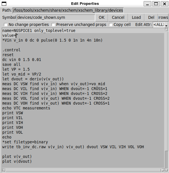
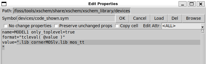
- The spice directives MODELS1 and NGSPICE1 are code.sym instances with the attributes shown in Figure 6 and Figure 7
- Click the Netlist button to create a netlist which will give us a
.spicefile and then click on Simulate button to run the simulation.
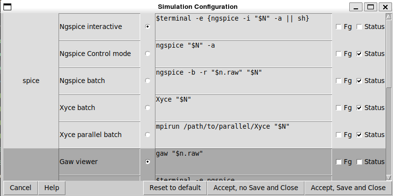
We have used NgSpice interactive mode for the spice simulation see Figure 8. We can also find other modes Simulation --> Configure simulator and tools
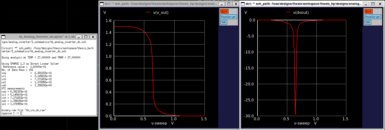
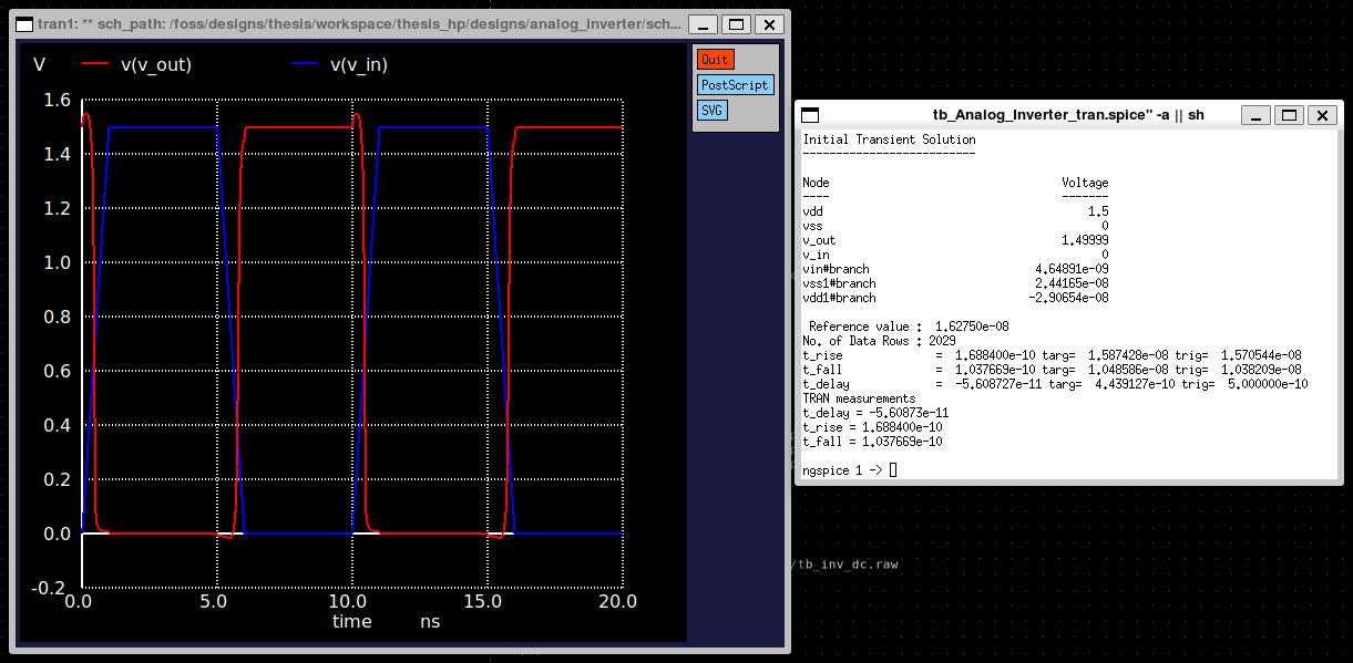
2.3 Output Results
Outputs of dc and transient analysis can be seen in
2.4 Post processing and simulation using python


2.5 Introduction to Layout
Layout is the physical representation of an integrated circuit, where circuit components such as transistors, interconnects, and vias are defined geometrically on various layers corresponding to materials used in fabrication. The layout must adhere strictly to design rules provided by the semiconductor foundry. We have two tools Magic and KLayout which enables layout design and verification. Magic being a long-standing tool favored for its tight integration with open-source flows, while KLayout offers powerful editing, scripting, and visualization capabilities, especially suited for hierarchical designs and PDKs such as SG13G2.
2.5.1 Designing Layout using Klayout
Layout design is performed using KLayout, an open-source layout viewer and editor for GDSII and OASIS files. Inverter layout can be built either manually from scratch or using parametric cells (P_Cells) from the IHP SG13G2 PDK, p_cells simplify device instantiation by allowing parameterized generation of transistors and other structures. KLayout supports precise layer control, design rule checking, and layout-versus-schematic (LVS) compatibility.
Start terminal and run IIC-OSIC docker image.
To select the PDK, use command
iic-pdk ihp-sg13grefer Figure 11
This step is crucial as it sets the technology IHP-SG13G2 in the tools.
- Start klayout amd refer Figure 12. A new window of Klayout will open after the command.
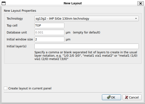
- To create new layout, Go to
Files >> New Layout. New Layout Properties dialog box will appear, changeTop Cell from TOP to inv(inverter)and leave the rest the same refer Figure 13
- Now go to
Basic - Basic Layout Objectson the left panel. UnderSG13_dev - IHP SG13G2 Pcells, select an NMOS device and place it in the layout.Press ESCto exit placement mode. Repeat the process for the PMOS, placing it directly above the NMOS to follow standard inverter structure.
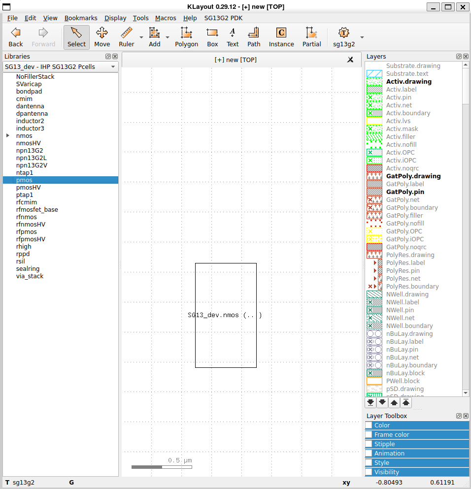
- On the right side, the layer list shows all available layers; bold entries indicate layers currently used in the layout. To view all layers from the full cell hierarchy,
click Display → Full Hierarchy | Press Shift + F.
To rotate a PCell, go to the Edit tab >> Move, select the PCell, then right-click. Use the mouse wheel to zoom in and out, and press the middle mouse button to pan the layout view.
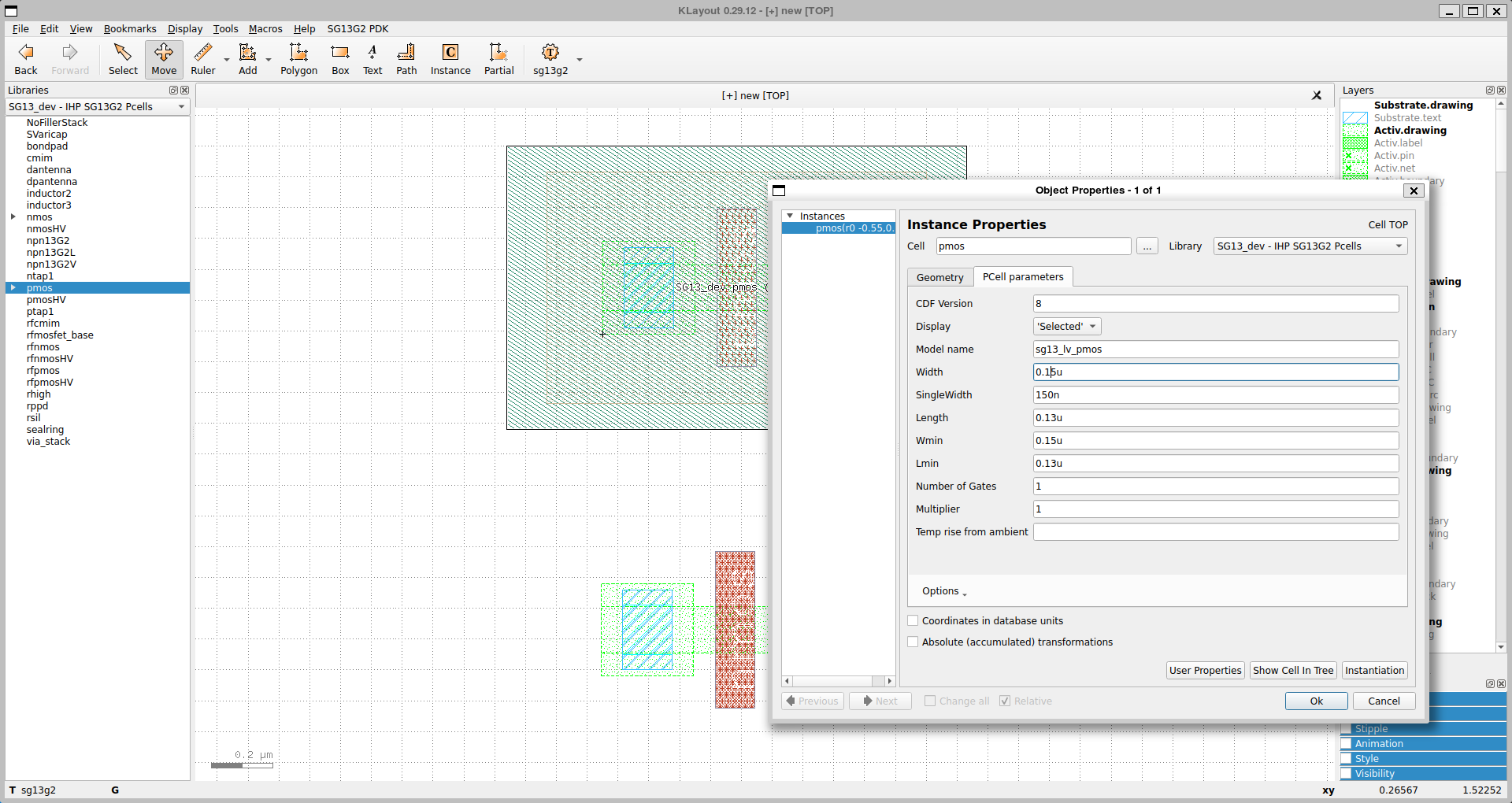
Double-click on the PCellto open its parameter editor. Set parameters like the width and length values to match those used in your Xschem schematic, thenclick OKto apply the changes refer Figure 15
Use the keyboard arrow keys to align the NMOS directly below the PMOS. Connect the input by joining the gates of both transistors using the
polysilicon layer - GatPoly.drawing. Connect the output by linking the source and drain of PMOS and NMOS with theMetal1 layer - Metal1.drawing. Similarly, useMetal1.drawingto connect the PMOS source to VCC and the NMOS source to VSS. Label all metal connections using theMetal1 pin layer - Metal1.pin. Refer to the IHP Open Source PDK DesignLIB documentation to verify the correct layer numbers and purposes.Finally, save your layout by going to
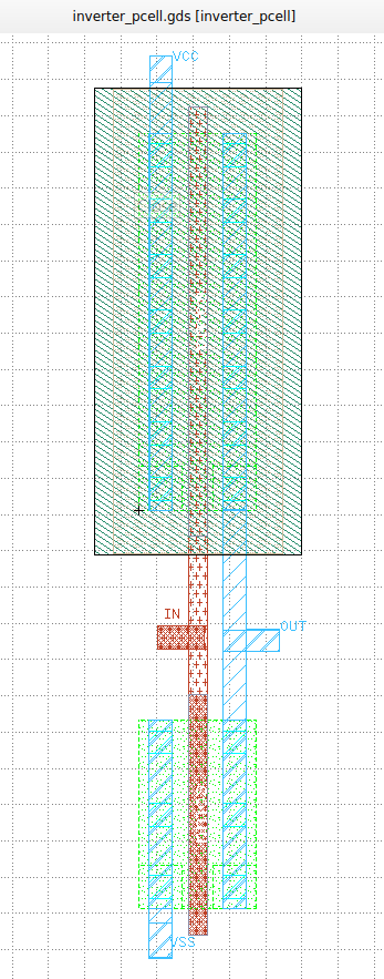
File → Save As, and choose theGDSIIformat to export your design. Your completed CMOS inverter layout should resemble the image shown below.
Here you can find all the layout rules in depth and with illustrations.
3 Klayout-PEX (KPEX)
While in the schematic, a connection between device terminals is seen as an equipotential, the stacked geometries in a specific layout introduce parasitic effects, which can be thought of additional resistors, capacitors (and inductors), not modeled by and missing in the original schematic.
To be able to simulate these effects, a parasitic extraction tool (PEX) is used, to extract a netlist from the layout, which represents the original schematic (created from the layout active and passive elements) augmented with the additional parasitic devices.
3.1 Why Do We Need PEX?
| Reason | Description |
|---|---|
| Performance Degradation | Parasitic capacitance reduces bandwidth and phase margin. |
| Offset and Mismatch Effects | Parasitic coupling causes imbalance in differential paths. |
| Stability Impact | Additional phase lag from parasitics can destabilize feedback loops. |
| Post-Layout Verification | Confirms that layout did not violate design intent (gain, UGB, PSRR, etc.). |
| Tapeout Confidence | Ensures high correlation between simulation and silicon behavior. |
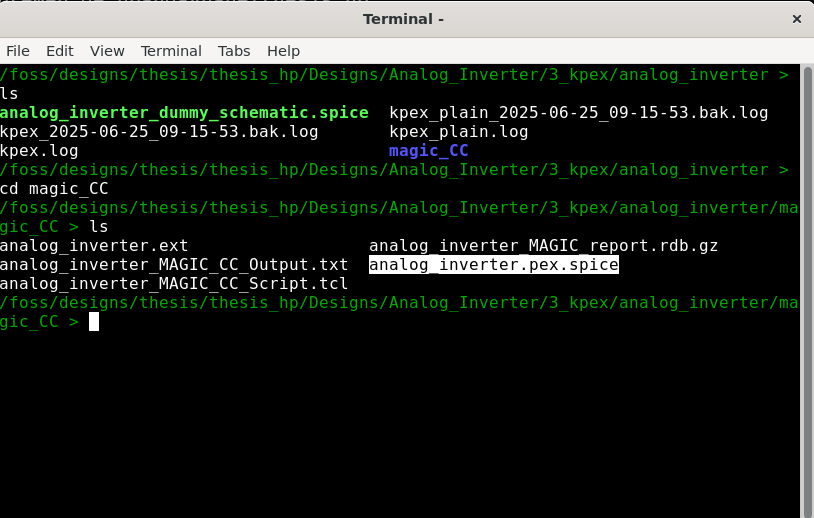
IIC-OSIC-Tools offers KPEX for this purpose which is a tool, well integrated with Klayout by using its API.
3.2 PEX using Klayout-PEX tool
IIC-OSIC-Tools comes with pre-installed tool called as K-pex. The current status of KLayout-PEX says as following:
Available KLayout PEX Engines:
| Engine | PEX Type | Status | Description |
|---|---|---|---|
KPEX/MAGIC |
CC, RC | Usable | Wrapper engine, using installed magic tool |
KPEX/FasterCap |
CC | Usable, pending QA | Field solver engine using FasterCap |
KPEX/FastHenry2 |
R, L | Planned | Field solver engine using FastHenry2 |
KPEX/2.5D |
CC | Under construction | Prototype engine implementing MAGIC concepts/formulas with KLayout means |
KPEX/2.5D |
R, RC | Planned | Prototype engine implementing MAGIC concepts/formulas with KLayout means |
3.3 Running the KPEX/MAGIC Engine
The magic section of kpex --help describes the arguments and their defaults. Important arguments:
--magicrc: specify location of themagicrcfile
--gds: path to the GDS input layout
--magic: enable magic engine--out_dir: set the output directory
3.3.1 Example Command
kpex --pdk ihp_sg13g2 --magic --gds GDS_PATH --out_dir OUTPUT_DIR_PATHmore to kpex can be found under the command kpex --help
/foss/designs > kpex --help
Usage: kpex [--help] [--version] [--log_level LOG_LEVEL]
            [--threads NUM_THREADS] --pdk {ihp_sg13g2,sky130A}
            [--out_dir OUTPUT_DIR_BASE_PATH] [--gds GDS_PATH]
            [--schematic SCHEMATIC_PATH] [--lvsdb LVSDB_PATH]
            [--cell CELL_NAME] [--cache-lvs CACHE_LVS]
            [--cache-dir CACHE_DIR_PATH] [--lvs-verbose KLAYOUT_LVS_VERBOSE]
            [--blackbox BLACKBOX_DEVICES] [--fastercap] [--fastcap] [--magic]
            [--2.5D] [--k_void K_VOID] [--delaunay_amax DELAUNAY_AMAX]
            [--delaunay_b DELAUNAY_B] [--geo_check GEOMETRY_CHECK]
            [--diel DIELECTRIC_FILTER] [--tolerance FASTERCAP_TOLERANCE]
            [--d_coeff FASTERCAP_D_COEFF]
            [--mesh FASTERCAP_MESH_REFINEMENT_VALUE]
            [--ooc FASTERCAP_OOC_CONDITION]
            [--auto_precond FASTERCAP_AUTO_PRECONDITIONER] [--galerkin]
            [--jacobi] [--magicrc MAGICRC_PATH] [--magic_mode {CC,RC,R}]
            [--magic_cthresh MAGIC_CTHRESH] [--magic_rthresh MAGIC_RTHRESH]
            [--magic_tolerance MAGIC_TOLERANCE] [--magic_halo MAGIC_HALO]
            [--magic_short {none,resistor,voltage}]
            [--magic_merge {none,conservative,aggressive}] [--mode {CC,RC,R}]
            [--halo HALO] [--scale SCALE_RATIO_TO_FIT_HALO]

kpex: KLayout-integrated Parasitic Extraction Tool

Special Options:
  --help, -h            show this help message and exit
  --version, -v         show program's version number and exit
  --log_level LOG_LEVEL
                        log_level ∈ {'all', 'debug', 'subprocess', 'verbose',
                        'info', 'warning', 'error', 'critical'}. Defaults to
                        'subprocess'
  --threads NUM_THREADS
                        number of threads (e.g. for FasterCap) (default is 48)

Parasitic Extraction Setup:
  --pdk {ihp_sg13g2,sky130A}
                        pdk ∈ {'ihp_sg13g2', 'sky130A'}
  --out_dir, -o OUTPUT_DIR_BASE_PATH
                        Output directory path (default is 'output')

Parasitic Extraction Input:
  Either LVS is run, or an existing LVSDB is used

  --gds, -g GDS_PATH    GDS path (for LVS)
  --schematic, -s SCHEMATIC_PATH
                        Schematic SPICE netlist path (for LVS). If none given,
                        a dummy schematic will be created
  --lvsdb, -l LVSDB_PATH
                        KLayout LVSDB path (bypass LVS)
  --cell, -c CELL_NAME  Cell (default is the top cell)
  --cache-lvs CACHE_LVS
                        Used cached LVSDB (for given input GDS) (default is
                        True)
  --cache-dir CACHE_DIR_PATH
                        Path for cached LVSDB (default is .kpex_cache within
                        --out_dir)
  --lvs-verbose KLAYOUT_LVS_VERBOSE
                        Verbose KLayout LVS output (default is False)

Parasitic Extraction Options:
  --blackbox BLACKBOX_DEVICES
                        Blackbox devices like MIM/MOM caps, as they are
                        handled by SPICE models (default is False for testing
                        now)
  --fastercap           Run FasterCap engine (default is False)
  --fastcap             Run FastCap2 engine (default is False)
  --magic               Run MAGIC engine (default is False)
  --2.5D                Run 2.5D analytical engine (default is False)

Fastercap Options:
  --k_void, -k K_VOID   Dielectric constant of void (default is 3.9)
  --delaunay_amax, -a DELAUNAY_AMAX
                        Delaunay triangulation maximum area (default is 50)
  --delaunay_b, -b DELAUNAY_B
                        Delaunay triangulation b (default is 0.5)
  --geo_check GEOMETRY_CHECK
                        Validate geometries before passing to FasterCap
                        (default is False)
  --diel DIELECTRIC_FILTER
                        Comma separated list of dielectric filter patterns.
                        Allowed patterns are: (none, all, -dielname1,
                        +dielname2) (default is all)
  --tolerance FASTERCAP_TOLERANCE
                        FasterCap -aX error tolerance (default is 0.05)
  --d_coeff FASTERCAP_D_COEFF
                        FasterCap -d direct potential interaction coefficient
                        to mesh refinement (default is 0.5)
  --mesh FASTERCAP_MESH_REFINEMENT_VALUE
                        FasterCap -m Mesh relative refinement value (default
                        is 0.5)
  --ooc FASTERCAP_OOC_CONDITION
                        FasterCap -f out-of-core free memory to link memory
                        condition (0 = don't go OOC, default is 2)
  --auto_precond FASTERCAP_AUTO_PRECONDITIONER
                        FasterCap -ap Automatic preconditioner usage (default
                        is True)
  --galerkin            FasterCap -g Use Galerkin scheme (default is False)
  --jacobi              FasterCap -pj Use Jacobi preconditioner (default is
                        False)

Magic Options:
  --magicrc MAGICRC_PATH
                        Path to magicrc configuration file (default is
                        '/foss/pdks/ihp-sg13g2/libs.tech/magic/ihp-sg13g2.magi
                        crc')
  --magic_mode {CC,RC,R}
                        magic_mode ∈ {'CC', 'RC', 'R'}. Defaults to 'CC'
  --magic_cthresh MAGIC_CTHRESH
                        Threshold (in fF) for ignored parasitic capacitances
                        (default is 0.01). (MAGIC command: ext2spice cthresh
                        <value>)
  --magic_rthresh MAGIC_RTHRESH
                        Threshold (in Ω) for ignored parasitic resistances
                        (default is 100). (MAGIC command: ext2spice rthresh
                        <value>)
  --magic_tolerance MAGIC_TOLERANCE
                        Set ratio between resistor and device tolerance
                        (default is 1). (MAGIC command: extresist tolerance
                        <value>)
  --magic_halo MAGIC_HALO
                        Custom sidewall halo distance (in µm) (MAGIC command:
                        extract halo <value>) (default is no custom halo)
  --magic_short {none,resistor,voltage}
                        magic_short ∈ {'none', 'resistor', 'voltage'}.
                        Defaults to 'none'
  --magic_merge {none,conservative,aggressive}
                        magic_merge ∈ {'none', 'conservative', 'aggressive'}.
                        Defaults to 'none'

2.5D Options:
  --mode {CC,RC,R}      mode ∈ {'CC', 'RC', 'R'}. Defaults to 'CC'
  --halo HALO           Custom sidewall halo distance (in µm) to override tech
                        info (default is no custom halo)
  --scale SCALE_RATIO_TO_FIT_HALO
                        Scale fringe ratios, so that halo distance is 100%
                        (default is True)

Environmental variables:

  Variable             Description
 ━━━━━━━━━━━━━━━━━━━━━━━━━━━━━━━━━━━━━━━━━━━━━━━━━━━━━━━━━━━━━━━━━━━━━━━━━━━━
  KPEX_FASTCAP_EXE     Path to FastCap2 Executable. Defaults to 'fastcap'
  KPEX_FASTERCAP_EXE   Path to FasterCap Executable. Defaults to 'FasterCap'
  KPEX_KLAYOUT_EXE     Path to KLayout Executable. Defaults to 'klayout'
  KPEX_MAGIC_EXE       Path to MAGIC Executable. Defaults to 'magic'
  PDKPATH              Optional (required for default magicrc), e.g.
                       $HOME/.volare
  PDK                  Optional (required for default magicrc), (e.g.
                       sky130A)
Once PEX is succesfully done, the extracted netlist SPICE file will be generated in the provided output path, which consists of extracted parasitics which can be further used to do post layout simulations and verify whether the design layout satisfies the design specifications or not.
3.4 Post layout simulation.
We have established testbenches for DC, AC, and transient analysis using the symbol of the designed inverter as a subcircuit. The next step is to perform post-layout simulation by replacing the schematic netlist with the extracted layout netlist (PEX), in order to verify whether the performance remains consistent after layout parasitics are included.
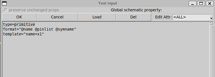
Firstly we need to open the symbol file in Xschem, edit the properties of the symbol See Figure 18. Change from subcircuit to primitive.
Once changed to primitive, now we can include the .spice file from PEX to the testbench. See Figure 19
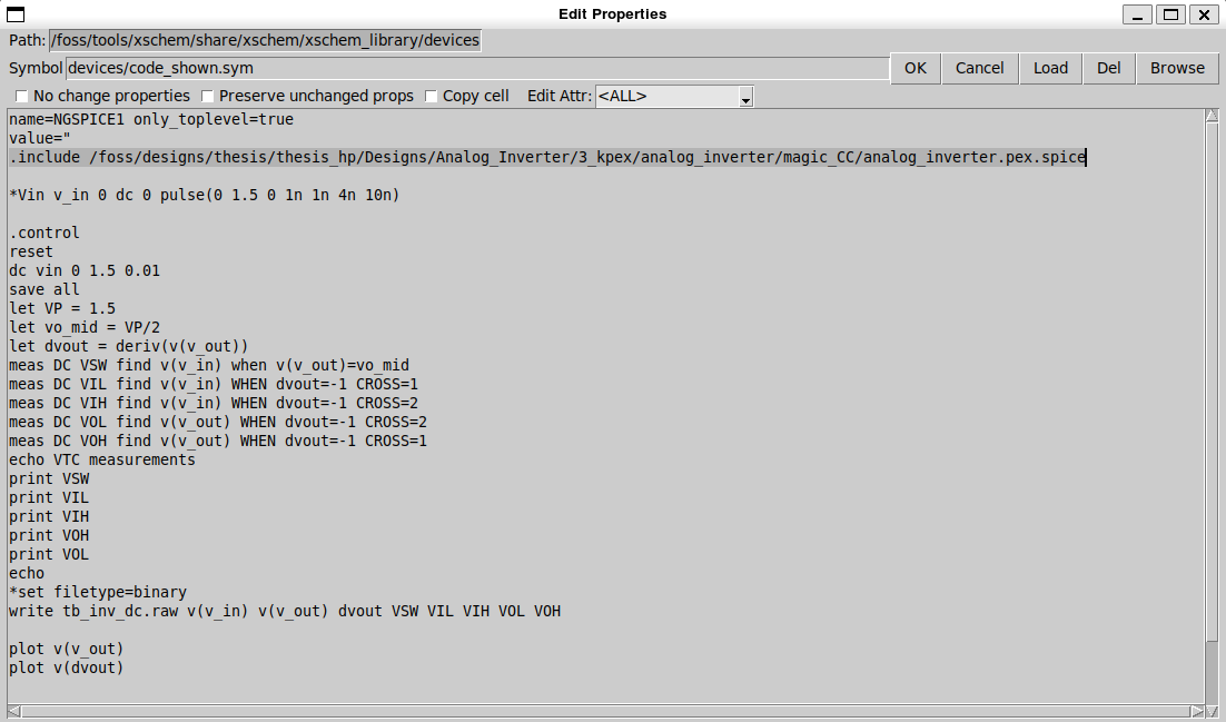
3.5 Results
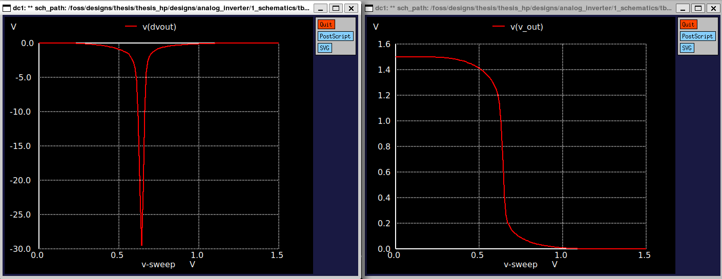
Figure 20 shows that the response is as same as we expected from our schematic.
4 Xschem Commands
Useful shortcuts are as follows
4.0.0.1 Moving around in a schematic:
Cursor keysto move aroundCtrl-eto go back to parent schematiceto descend into schematic of selected symbolito descend into symbol of selected symbolffull zoom on schematicShift-zto zoom inCtrl-zto zoom out
4.0.0.2 Editing schematics:
Delto delete elementsInsto insert elements from libraryEscapeto abort an operationCtrl-#to rename components with duplicate namescto copy elementsAlt-Shift-lto add wire labelAlt-lto add label pinmto move selected objectsShift-Rto rotate selected objectsShift-Fto mirror / flip selected objectsqto edit propertiesCtrl-sto save schematictto place a textShift-Tto toggle theignoreflag on an instanceuto undo an operationwto draw a wireShift-Wdraw wire and snap to close pin or net point&to join, break, and collapse wiresAto make symbol from schematicAlt-sto reload the circuit if changes in a subcircuit were made
4.0.0.3 Viewing/Simulating Schematics
5to only view probeskto highlight selected netShift-Kto unhighlight all netsShift-oto toggle light/dark color schemesto run a simulationa & bto add cursors to an in-circuit simulation graphffull zoom on y- or x-axis in in-circuit simulation graph
5 ngspice Commands
Useful shortcuts are as follows:
5.1 Commands
ac dec|lin points fstart fstopperforms a small-signal ac analysis with either linear or decade sweepdc sourcename vstart vstop vincr [src2 start2 stop2 incr2]runs a dc-sweep, optionally across two variablesdisplayshows the available data vectors in the current plotechocan be used to display text,$variableor$&vector, can be useful for debugginglet name = exprto create a new vector;unlet vectordeletes a specified vector; access vector data with$&veclinearize veclinearizes a vector on an equidistant time scale, do this before an FFT; withset specwindow=windowtypea proper windowing function can be setmeascan be used for various evaluations of measurement results (see ngspice manual for details)noise v(output <ref>) src (dec|lin) pts fstart fstopruns a small-signal noise analysisopcalculates the operating point, useful for checking bias points and device parametersplot expr vs scaleto plot somethingprint exprto print it, useprint allto print everythingremzeroveccan be useful to remove vectors with zero length, which otherwise cause issues when saving or plotting datarusageplot information about resource usage like memorysave allorsave signalspecifies which data is saved during simulation; this lowers RAM usage during simulation and size of RAW file; do save before the actual simulation statementsetplotshow a list of available plotsset var = valueto set the value of a variable; use variable with$var;unset varremoves a variableset enable_noisy_rto enable noise of behavioral resistors; usually, this is a good ideashell cmdto run a shell commandshow : param, likeshow : gmshows the \(g_m\) of all devices after running an operating point withopspecplots a spectrum (i.e. frequency domain plot)statusshows the saved parameters and nodestfruns a transfer function analysis, returning transfer function, input and output resistancetran tstep tstop <tstart <tmax>>runs a transient analysis untiltstop, reporting results withtstepstep size, starting to plot attstartand performs time steps not larger thentmaxwrdatawrites data into a file in a tabular ASCII format; easy to further processwritewrites simulation data (the saved nodes) into a RAW file; default is binary, can be changed to ASCII withset filetype=ascii; withset appendwritedata is added to an existing file
5.2 Options
Use option option=val option=val to set various options; important ones are:
abstolsets the absolute current error tolerance (default is 1pA)gminis the conductance applied at every node for convergence improvement (default is 1e-12); this can be critical for very high impedance circuitsklusets the KLU matrix solverlistprint the summary listing of the input datamaxordsets the numerical order of the integration method (default is 2 for Gear)methodset the numerical integration method togearortrap(default istrap)nodeprints the node tableoptsprints the option valuestempsets the simulation temperaturereltolset the relative error tolerance (default is 0.001 = 0.1%)savecurrentssaves the terminal currents of all devicessparsesets the sparse matrix solver, which can run noise analysis, but is slower thankluvntolsets the absolute voltage error tolerance (default is 1µV)warnenables the printing of the SOA warning messages
5.3 Convergence Helper
option gmincan be used to increase the conductance applied at every nodeoption method=gearcan lead to improved convergence.nodesetcan be used to specify initial node voltage guesses.iccan be used to set initial conditions